Connect POI substrates
Tailored multilayers piezoelectric substrates enable high-performance RF filters with best-in-class uniformity, thanks to Smart Cut™ technology.

Let us help make your project a success
Connect Piezoelectric Materials on Insulators

Fusing its elastic wave components expertise with its Smart Cut™ technology, Soitec has developed MultiLayer piezoelectric substrates addressing the demanding RF filters market based on Surface Acoustic Wave technology.
The Connect POI substrate, Piezoelectric On Insulators substrate, combined with InterDigital Transducers, enables the creation of high-performance SAW filters that meet the demands of stringent telecommunication bands by offering improved RF performance through a higher quality factor (Q) and lower insertion losses (IL). Additionally, it provides better thermal properties, including a low temperature coefficient of frequency (TCF) and enhanced thermal dissipation. The substrate also supports flexible bandwidth thanks to an appropriate acoustic coupling factor (k²), well-matched phase velocity, and multiplexing capability. Furthermore, it is well-suited for high-volume manufacturing: it offers robustness and compatibility with advanced package and assembly flows for Front-End modules.
Connect POI portfolio
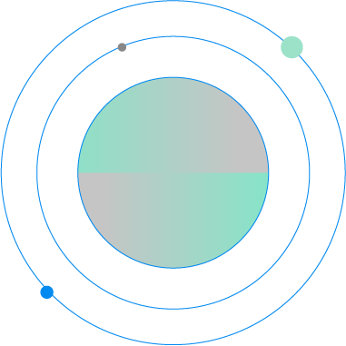
Connect POI description
The multilayers Connect POI substrate is composed of four layers. Used piezoelectric materials are Lithium Tantalate LiTaO3 and Lithium Niobate LiNbO3.
LT6-MHB product
150 mm wafer size addressing the RF Filter Mid High Band segment, from 1 to 3+ GHz.
Multiple Silicon orientations and Euler Angles are available.
LT6-LB product
150 mm wafer size addressing the RF Filter Low Band segment, below 1 GHz.
Multiple Silicon orientations and Euler Angles available.
LN6 product
150 mm wafer size with LiNbO3 , addressing wider RF bands of the RF Filter segments, up to 3+ GHz.
LT8-MHB & LT8-LB products
200 mm wafer size addressing the RF Filter Mid High Band and Low Band segments, up to 3+ GHz.
Connect POI boosts the communications speed & rate between connected equipments, reducing the consumption
The versatile Connect POI substrate offers the options to tailor the type of filter skirt of any 5G New Radio band, for any data rate and speed. Coexistence in a massive connected network is not an issue anymore. Nor the integration into compact systems. Connect POI even enables multiplexing to filter several bands on the same die. It also empowers the communication system to lower consumption for data transmission, serving ideally the 5G smartphone and tablet battery life.
Connect POI technology makes the bluetooth integration into smartglasses possible : it enables coexistence with the increased allocation of 5G bands thanks to high-selectivity filters ! Moreover, the ML-SAW filter on POI is very compact. Moreover, the ML-SAW on POI enables the whole telecommunication channel to work with a lower consumption : perfect for those bright glasses to stay light and longer, with the objective of achieving one operating day without charge-in!
Whatever the accuracy requested, for autonomous car or smartphone positioning, the filter needs to segregate the Global Navigation Satellite System (GPS, Glonass, Galileo, BeiDou, NavIC, QZSS) tracking signal from any other transmitted telecommunication. Selectivity, isolation, and low consumption are the Connect POI features enabling this ! Achievable miniaturization is an additional benefit for the wearable market !
Highlights
Gain for Tx filters
SAW-ladder— and impedance element filters —, built from series and parallel resonators, take full advantage of POI substrates, where maximized Q factors and ideal coupling deliver steep filter skirts and ultra- low insertion loss. These architectures are well suited to handle maximum incident power. With the Connect POI product, thermal compensation comes from the substrate, there’s no need for an additional deposited layer. Moreover the whole POI structure fosters heat dissipation, responding to the Power Class 1.5 requirements. And no issue with the 50 ohms matching.
Gain for Rx filters
Connect POI empowers DMS, Double Mode SAW, and innovative architectures, as it offers extremely low Insertion Loss and out-of-band attenuation options. Demanding specifications of Rx filters can be reached, responding to Adjacent Channel Rejection and Adjacent Channel Selectivity requirements. Advantages listed for the Tx filters are also applicable for the Rx filters
Multiplexing, from duplexer to x-plexer
Duplexer can be designed by combining the both previous approaches of Rx and Tx filters on POI. The Connect POI versatility enables also to integrate, on a same die, some filters addressing different frequencies: diplexer and multiplexer can be then integrated on a single chip, with a single IDT metal layer. Reached cross-isolation or isolation across bands is sufficient between the aggregate paths.
Ease of filter manufacturing and assembly
The compatibility with multiple IDT technology variants, and advanced package technologies, makes the Connect POI MultiLayer RF Filter easy to produce and integrate. Just a few litho-masks are needed for this process. The Si handle robustness enables the application of advanced packaging technologies, such as fine WLCSP, flip-chip, followed by module assembly, and System In Packages for RFFE modules. One advantage stands in the achievable yields, much better than with TC-SAW technology, particularly for multi-frequency devices.
Advantages of a SAW on POI compared to a SAW on piezoBulk
The POI multilayers stack offers better waveguide performances, boosting the piezoelectric properties, and limiting its thermoelastic variations. All, on a robust mechanical substrate ! Moreover a substrate stack can be designed to optimize performance across various frequency bands, enabling efficient multiplexing !
5G bands selectivity & coexistence with WiFi
Connect POI is capable of addressing the whole spectrum, including LTE, 5G, and beyond, enabling energy efficient RF filter designs with compact footprint. Which leads to address multiple markets : Mobile Market,IoT Market,Non Terrestrial Network and SATCOM.
Learn more about Connect POI
Frequently asked questions
What is a RF Filter?
A RF Filter enables to sort out the signal of interest, without interference, among a growing demand of transmission and reception signals.
The RF filter is the first function next to the antenna. It is also present on the whole RX / TX receive/transmit channel, specific to each telecommunication standard, such as GSM, 5G, GNSS, NTN,....
The RF filter is the first function next to the antenna. It is also present on the whole RX / TX receive/transmit channel, specific to each telecommunication standard, such as GSM, 5G, GNSS, NTN,....
What is a POI substrate? What is POI?
POI stands for Piezoelectric On Insulator substrate.
Typically, a piezoelectric material is bonded on a Silicon substrate, using a silicon dioxide layer at the interface. It is a wafer technology enabling better acoustic filtering performances than bulk materials.
Connect POI is the Soitec’s POI substrate optimized to boost performances of SAW on POI.
What is piezoelectric effect ?
Piezoelectricity is a reverse phenomenon of physics that converts mechanical energy into electrical one. Piezoelectric materials are commonly used for RF Filter applications, using two main technologies : Bulk Acoustic Wave, called BAW, and Surface Acoustic Wave, called SAW.
What is SAW on POI?
SAW stands for Surface Acoustic Wave. It is, with the Bulk Acoustic Wave, one of the two types of waves used in acoustic filters, to address the market demand for high compactness passive filters.
SAW on POI filters are composed of metallic InterDigital Transducers, patterned on a POI substrate. The selected wave energy is confined within the top layer.
SAW on POI filters are composed of metallic InterDigital Transducers, patterned on a POI substrate. The selected wave energy is confined within the top layer.
What are the advantages of a SAW on POI versus a SAW on piezoBulk?
The POI multilayers stack offers better waveguide performances, boosting the piezoelectric properties, and compensating for its thermoelastic variations. All, on a robust mechanical substrat. Multiplexing is achievable thanks to the versatility of the whole POI multilayers substrate.
What is a Trap Rich layer?
Trap Rich or TR layer refers to a polysilicon layer with high density of traps that captures free carriers forming undesirable parasitic conduction. It enables a much better RF linearity at any point of the filter IC.
Related Events
Silicon Photonics Workshop at ECOC 2026
-
ICSCRM 2026
Related Content
Mobile Communications
Soitec’s semiconductor substrates enable energy-efficient, reliable, and secure data acquisition, processing, and communication for the mobile communications market.
Beyond Silicon
Soitec is diversifying beyond silicon technologies by exploring and advancing new material solutions.
Smart Cut™
An electronics industry standard for engineered substrates manufacturing.