Smart Cut™ Technology
An electronics industry standard for engineered substrates manufacturing

Ready to join us and build your future?
Soitec offers its customers substrate solutions where each layer is optimized for the needs of the application : precise thickness, insulation, functional layer, mechanical support, transparency, etc. Each characteristic of the wafer is obtained without compromise for minimized energy consumption and maximum performance.
The source of this cutting-edge technological adventure is at CEA Leti. Where researchers have developed an original crystalline layer transfer method: Smart Cut™, allowing for the first time to have a crystalline layer on any type of support. Pushing the mastery of this technology to the extreme, Smart Cut™ has gradually established itself as the reference technique for transferring thin crystalline layers, to the point of making it a standard in the electronics industry.
A scalpel on an Atomic scale

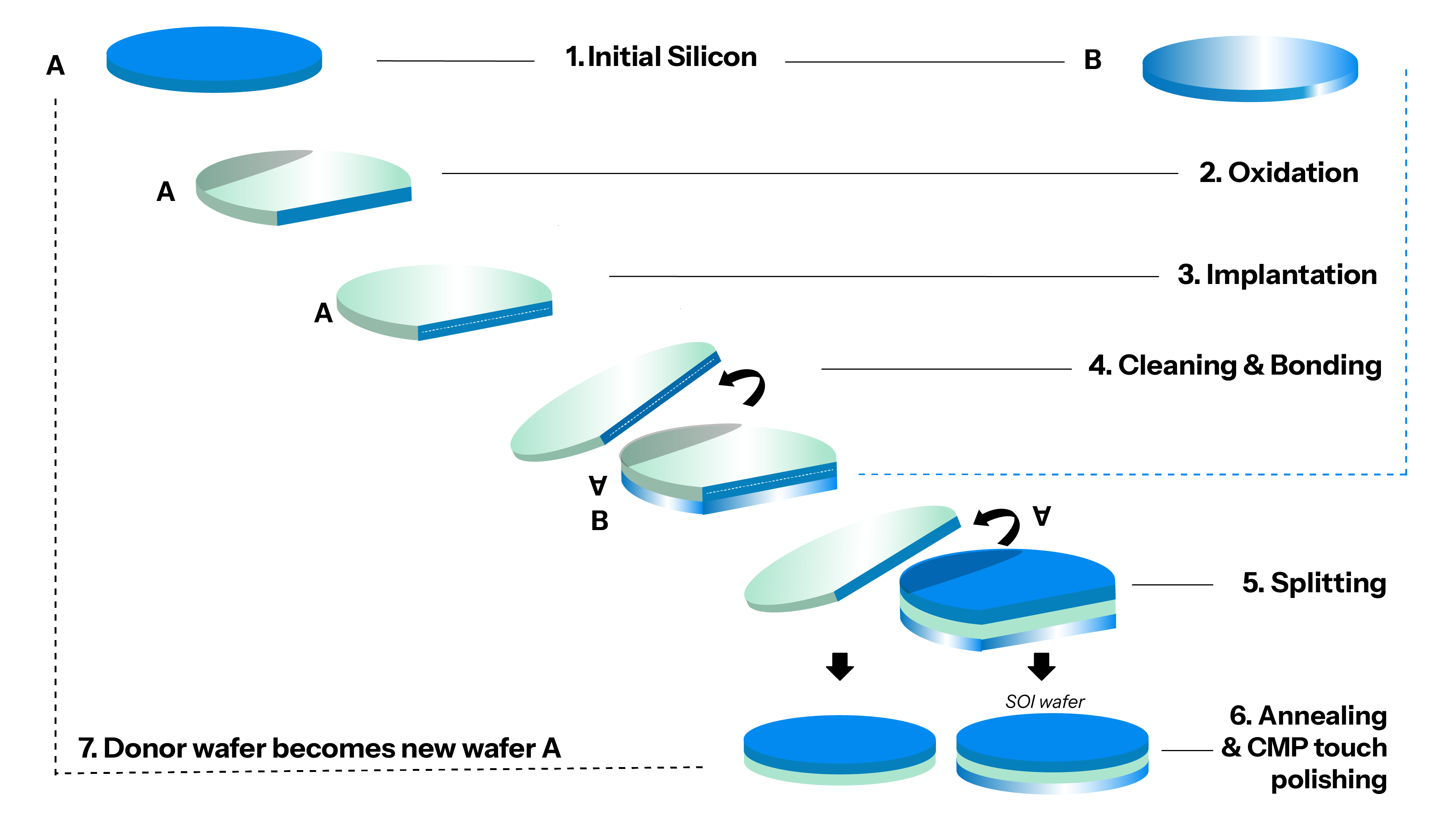
Smart Cut™ technology is based on the combination of light ion implantation and molecular adhesion bonding to transfer ultrathin single crystal layers from one substrate to another. It works like a scalpel on the atomic scale and allows you to position a crystalline layer of perfect quality on all types of materials.
Smart Cut™ allows us to generate the active layers of our structures independently of the mechanical support substrate, and any functional layers that can be inserted.
This combination of implantation and bonding of plates has numerous advantages:
- Ion implantation makes it possible to obtain high quality, very uniform transferred layers.
- The thickness of the transferred layer can be determined with extreme precision by adjusting the implantation energy.
- Plate bonding is applicable to different materials and a wide range of temperatures, paving the way for innovative alternatives when thermal expansion rules out the possibility of deposition.
- The donor substrate can be recycled repeatedly; after each layer transfer, the surface is refreshed and the substrate can be reused.
Numerous industrial advantages
Smart Cut™ technology is particularly well suited to high volume production:
- It is based on standard tools from the semiconductor industry and can adapt to wafers of different diameters.
- The range of potential thicknesses of the silicon top layer and buried oxide layer provides immense flexibility.
- It makes it possible to obtain very high quality, in terms of uniformity and bonding interfaces, but also unrivaled control of thickness variability.
.jpg?sfvrsn=7096cfc8_1&Width=1300&Height=500&ScaleUp=false&Quality=High&Method=CropCropArguments&Signature=FBC32612C6E78479E81DAD63310B61C06360C77B)
Limitless innovation opportunities
Combined with other materials and other Soitec technologies, Smart Cut™ makes it possible to transfer a thin film of a monocrystalline material to any other material, while retaining its initial crystallographic properties.
With these technologies, we are able to offer players in the electronics industry new opportunities for innovation and differentiation in areas of microelectronics as varied as sensors, silicon photonics, power electronics, advanced CMOS nodes, 3D hybrid integration, radio frequency electronics, ultra-low power electronics, etc.
The applications are multiple: wireless & 5G communication, electric and autonomous vehicles, edge computing, connected objects, augmented reality and artificial intelligence.
Related Content
RF-SOI
Our RF-SOI substrates deliver reliable RF performance and value for high-growth, high-volume cellular, Wi-Fi and other connectivity markets.
FD-SOI
Soitec's FD-SOI substrates make the world of smart devices, automotive radar and processors and RF mmWave.
POI
Tailored multilayers piezoelectric substrates that create high performance RF filters, with best-in-class uniform thin films, thanks to the Smart Cut™ technology.

