Photonics-SOI substrates
Advanced solutions enable high data rates with optimized cost across a wide range of datacom applications

Let us help make your project a success
Photonics-SOI delivers high speed and energy efficiency in optical interconnects

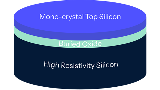
Photonics-SOI from Soitec is an advanced technology platform that integrates photonic components on a silicon-on-insulator (SOI) substrate to enhance optical communication capabilities.
Photonics-SOI offers significant advantages for optical transceivers, including high data rates, cost efficiency, power savings, compact size, and improved signal integrity. These benefits make it a compelling choice for high-speed data center interconnect applications.
Photonics-SOI provides several advantages for personal healthcare sensors, including miniaturization, cost efficiency, high sensitivity, and integration capabilities. These benefits enable the development of advanced, compact, and accurate monitoring devices for health applications.
Photonics-SOI is used in Light Detection and Ranging (LiDAR) devices which are increasingly being used in Advanced driver-assistance system (ADAS), mobile and consumer applications.
Photonics-SOI enables the implementation of Quantum Key Distribution (QKD), a method for secure communication based on quantum principles. Silicon-based photon sources and detectors can be used to create and distribute quantum keys between parties, ensuring secure data transmission.
How Photonics-SOI will impact your products
Enhanced Bandwidth and Speed
The technology supports high-bandwidth and high-speed optical communication, addressing the increasing demands for data transfer in data centers, telecommunications, and computing systems.
Integration and scalability
By leveraging silicon’s established manufacturing processes, Photonics-SOI supports scalable production and seamless integration with existing silicon electronics, facilitating the development of compact, high-density optical systems.
Reduced power consumption
Photonics-SOI contributes to lower power consumption by utilizing optical signals for data transmission, which is more energy-efficient than traditional electrical interconnects, especially over long distances.
Where Photonics-SOI technology is being used
Soitec provides innovative solutions for high speed and robust connectivity in data center interconnect and network infrastructure connectivity. By offering superior thermal management and reduced power consumption, Soitec's substrates help optimize the operation of servers and networking devices, enabling faster data processing and lower energy usage.
Soitec offers a portfolio of solutions which enhance the performance and efficiency of Edge AI and IoT applications. By providing high-quality, energy-efficient substrates, Soitec helps to optimize IoT devices by enhancing their reliability and extending battery life, making them ideal for real-time data processing and communication in various applications.
Soitec empowers electric and autonomous vehicle innovation. Our industry-leading engineered substrates enable the development of advanced automotive applications, delivering superior energy efficiency, performance, robustness, integration, sustainability, faster time-to-market and intelligence.
Soitec empowers smart industrial applications and enables industry leading industrial automation. Our industry-leading engineered substrates enable the development of advanced industrial applications, delivering superior energy efficiency, performance, robustness, integration, sustainability, faster time-to-market and intelligence.
Current world’s semiconductor capacity and the demonstrated large scale manufacturability of engineered substrates have provided the possibility for every person in the world to afford at least one device - a smartphone for most - able to acquire, process and communicate information of its surroundings. As the leader in engineered substrates, Soitec is helping enterprising customers and partners in ensuring that their products meet the ever-increasing expectations in consumers' Quality-of-Experience. Our engineered substrates help ensure end-to-end energy efficiency, fast, secure and reliable data acquisition and processing and robust broadband connectivity.
Frequently asked questions
Photonics-SOI is used in a wide range of applications from data center interconnect, LiDAR, personal healthcare to quantum technologies.
Photonics-SOI offers the advantages of enhanced bandwidth and speed, higher integration and scalability, and reduced power consumption.
Related Events
SEMICON South East Asia 2026
IMS 2026
PCIM 2026
Related Content
Internet of Things (IoT)
Boosting IoT and Edge Computing through more intelligence and reduced energy consumption.
Cloud AI & Network Infrastructure
Soitec’s products enable high speed connectivity for Cloud AI and digital processing for the network infrastructure requirements.
Smart Cut™
An electronics industry standard for engineered substrates manufacturing.

