Group
Inside a world leader in innovative semiconductor materials
Empowering the world with smarter semiconductors
Soitec’s unique semiconductor materials power billions of everyday lives. Designed and manufactured with precision, they deliver a significant performance edge over microchips based on generic silicon wafers and other alternatives.
Soitec’s engineered substrates are driving the AI revolution—unlocking higher performance, lower latency, and greater energy efficiency. They also enhance user experience and strengthen data privacy, shaping a smarter and more sustainable future.

Soitec's vision
To be the undisputed sustainable leader in engineered substrates supplying the world with energy efficient semiconductors.
Ready to join us and build your future?
At the core of innovation
Soitec powers the world’s biggest technological revolutions—mobile communications, electric mobility, AI, smart devices…
With superior performance and energy efficiency, their advanced semiconductor materials are at the heart of fast-growing applications like AI or electric vehicles. In mobile communications, they’ve already set the global standard.
Mobile Communications
Empowering seamless and reliable connections to keep the world moving forward.
Automotive & Industrial
Empowering smarter, safer, and more sustainable vehicles and industries everywhere.
Edge & Cloud AI
Shaping the future with cutting-edge intelligence from the edge to the cloud.
Global leader with French roots

Thanks to its technological edge and unique position in the value chain, Soitec has become an essential global semiconductor player, recognized across the industry.
From its French roots, the company has grown internationally and now also manufactures in Singapore.
Sustainable by design

How Soitec drives innovation in the electronics value chain
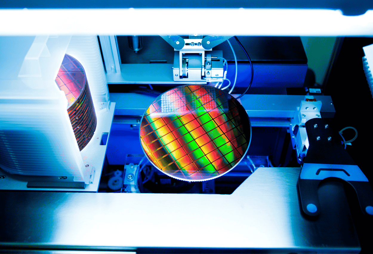
Soitec partners with leading silicon manufacturers to source raw wafers, meticulously crafted through smelting, casting, and cutting. Using the revolutionary Smart Cut&trade process, developed in the heart of Grenoble’s innovation hub, Soitec leverages nanotechnology at an atomic scale to create silicon-on-insulator (SOI) wafers.
This cutting-edge technology introduces an insulating layer between two silicon oxide layers, enhancing energy efficiency and boosting performance. By simplifying device architecture, SOI wafers also lower manufacturing costs, driving both innovation and sustainability in electronic components.
With its Smart Cut™ process, Soitec enables integrated circuit manufacturers to develop next-generation microelectronics that power a smarter, more energy-efficient future.
A unique business model to set an industry standard
Soitec has the largest industrial manufacturing site for SOI wafers (200 mm to 300 mm) in the world. It includes 4,500 m² of cleanrooms spread out between its three factories in France. In 2015, Soitec partnered with the Chinese company Simgui to manufacture 200-mm SOI wafers for the Chinese market and operate as a manufacturing partner (foundry model) for Soitec customers outside of China. Soitec also has a FD-SOI pilot line in Singapore.
The company introduced the Smart Cut™ technology on the market on an industrial scale, which today is used to make nearly all SOI wafers sold in the world. Soitec has licensed SOI technology to several leading wafer manufacturers including the Japanese company Shin-Etsu Handotai (SEH) in 1997 which continues to this date as well as to Simgui for manufacturing and selling certain 150 mm and 200 mm SOI products to Soitec exclusively.

Soitec at a glance
of turnover dedicated to R&D
+ 4,300
active patents
(for FY'25)
The governance
.jpg?sfvrsn=d6cc7a0d_3)
Soitec has been listed on the Euronext Paris market since 1999. Supported by shareholders, they pursue a policy of sustainable growth driven at the highest level of the company by an experienced, diverse and committed team
Related Content
Governance
Commitments
To contribute to a more sustainable future, we have placed environmental, social and governance issues at the heart of our strategy.
People

